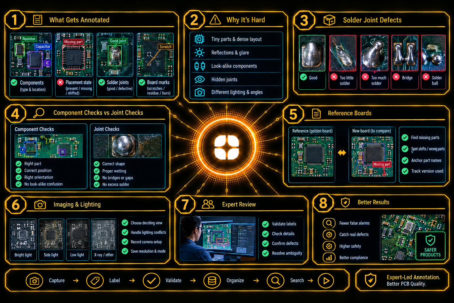
A circuit board can hold thousands of parts and tens of thousands of solder joints, many smaller than a grain of rice. One weak joint or missing part can make a device fail. Cameras check boards on the line, and AI helps decide which to pass, rework, or reject.
AI learns from labeled images. Good PCB inspection annotation means marking parts and joints the same way every time. This post explains what the work covers, why it is hard, and what manufacturing AI training data needs to get right.
Annotation for board images usually has four parts:
Models trained on these labels can flag a faulty board, point to the exact spot, and show which defects keep returning.
Boards are small, dense, and shiny.
Annotators need rules for images where a joint cannot be judged. A “good” label on a glare-covered joint teaches the model a false lesson.
A good joint has a smooth, shiny, evenly shaped fillet that wets the pad and the pin. Defects change that shape.
Each type needs a written definition, an example, and its closest look-alike. A rule should say how to label a joint with two flaws, and when a small bead counts as a defect and not just residue.
These two jobs look related but fail in different ways.
Component checks ask whether the right part sits in the right place, facing the right way. Labelers compare the board to its design, and errors come from look-alike parts and hard-to-read markings. Joint checks ask whether the solder is sound. Labelers judge shape, shine, and spread, and errors come from glare and from tiny differences between a good joint and a weak one.
A single guide for both would blur these differences. Each needs its own definitions, examples, and reviewers.
A reference board, also called a golden board, is a known-good example of the product. Annotators compare each image to it, which makes missing, shifted, or wrong parts easier to catch. It also anchors part names and positions, and helps separate real defects from normal variation, such as an approved part from another supplier.
Record which reference version each batch used. When a design changes, the reference must change, and older labels may need review.
Board machines often use several lights and angles, so one joint may have multiple views. A joint that looks dull under one light can look fine under another. The guide should say which view decides the label and how to treat conflicts. Record the camera, lighting mode, and resolution with each image, so teams can see whether errors come from the labels or the imaging.
Most boards are good, so serious defects are rare. Count examples for each defect type and component family, collect more of the thin ones early, and keep hard cases in a separate test group. Keep images from the same board, panel, or production run on one side of the train and test split, or scores will look better than they are.
Some joints cannot be judged from the image. Give annotators a “cannot judge” option and send doubtful cases to an expert. A false alarm slows the line, while a missed defect may reach a customer, so the rules should say how each is handled. We cover similar rules for another joining process in our guide to weld inspection imagery annotation.
People with electronics assembly experience know what a healthy joint looks like, how a bridge differs from a stray bead, and which parts are often mistaken for each other. They can tell a real flaw from a lighting effect.
Specialists write the defect definitions, set severity rules, and review hard cases. This reflects Globik AI’s approach of using verified domain experts for work that depends on judgment, where a generalist would be guessing.
Before starting a board inspection project, settle these points:
A circuit board packs thousands of small decisions into one image, so the labels must be exact and honest. Strong PCB inspection annotation uses clear defect definitions, versioned reference boards, rules for lighting and views, and reviewers who know how joints fail. With that foundation, models can help inspectors catch faulty boards before they ship.
It is the labeling of circuit board images so AI can find components and flag defects such as missing parts or weak solder joints. Annotators follow written rules based on the product design.
It is marking each solder joint as good or defective and naming the flaw, such as a bridge, too little solder, or a lifted pin. Each type needs a clear definition and example.
A reference board is a known-good example of the product. Annotators compare images against it to spot missing, shifted, or wrong parts, and teams record which version each batch used.
Parts are tiny and crowded, and glossy solder creates glare that hides or fakes defects. Clear rules and a cannot-judge option keep guesses out of the data.
Specialists know what healthy joints look like and which parts are often confused. They write clear defect rules and review doubtful images.